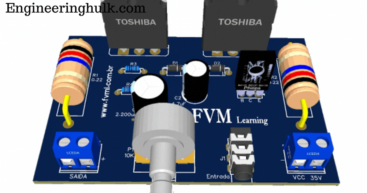
A power transistor is a transistor built to switch or control large currents (from a few amperes to thousands in modules) at high voltages (tens of volts to several kilovolts), and in power electronics it is used almost always as an on/off switch. The three power transistors are the power BJT, the power MOSFET and the IGBT. The MOSFET dominates low-voltage, high-frequency work, the IGBT dominates medium and high voltage, and the power BJT is now mostly found in older designs.
What makes a transistor a power transistor?
A small-signal transistor in an audio preamp handles milliamps. A power transistor has to block the full supply voltage when off, carry the full load current when on, and dissipate the heat of both switching and conduction losses. That changes its construction:
- Vertical structure. Current flows from the top surface down through the chip to the back, so the whole die area carries current.
- Thick, lightly doped drift region. This layer (n−) supports the blocking voltage. The higher the voltage rating, the thicker it must be, which is why high-voltage devices have more on-state loss.
- Large die and heavy packages. TO-220, TO-247 and press-fit or baseplate modules, mounted on heat sinks.
- Operated as a switch. Fully on (low voltage drop) or fully off (almost no current). Spending time in the active region would burn far too much power.
Unlike the thyristor family, all three power transistors can be turned off by their control terminal at any moment. That is their main advantage over the SCR; for the thyristor side of power electronics, see thyristor in power electronics.
Power BJT
Structure
A power BJT is usually an n+-p-n−-n+ device: emitter, base, a lightly doped collector drift region and a heavily doped collector contact. The emitter is split into narrow interdigitated fingers so that base current reaches all of it evenly.
How it switches
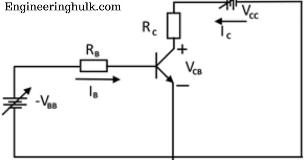
It is a current-controlled device. Base current IB drives it into saturation, where VCE(sat) is low (around 1 to 2 V). The problem is gain: a high-voltage power BJT may have a current gain of only 5 to 20, so a 50 A collector current can need 3 to 10 A of base current. Darlington pairs raise the gain but also raise the on-state drop. Turn-off is slow because stored charge in the base and drift region must be removed, which limits switching to a few kHz in practice.
Weak points
BJTs suffer from second breakdown: current crowds into a hot spot, and because the BJT’s resistance falls with temperature, that spot gets hotter still until the device fails. This also makes paralleling BJTs difficult.
Power MOSFET
Structure
Most power MOSFETs are vertical n-channel devices (VDMOS or trench MOSFETs) made of thousands of small cells in parallel on one chip. The gate is insulated from the silicon by a thin oxide layer, and the drain is at the back of the die. The structure contains an inherent body diode between source and drain, which conducts in reverse and is used as a freewheeling diode in many circuits.
How it switches
It is voltage-controlled. Raising the gate-source voltage above the threshold (typically 2 to 4 V; driven at 10 to 15 V for full enhancement) forms a channel. The gate draws current only to charge and discharge its capacitance, so the driver is simple. There is no minority-carrier storage, so the MOSFET switches in tens of nanoseconds, and silicon MOSFETs run from tens of kHz to above 1 MHz.
Strengths and limits
When on, a MOSFET behaves like a resistance RDS(on). RDS(on) rises with temperature, so parallel devices share current naturally and there is no second breakdown. The catch is that RDS(on) climbs steeply with voltage rating, which is why silicon MOSFETs are most attractive below a few hundred volts. Silicon carbide (SiC) MOSFETs push this limit to 1,200 V and beyond and are now common in electric-vehicle inverters and fast chargers.
IGBT (insulated gate bipolar transistor)
Structure
The IGBT looks like a power MOSFET with an extra p+ layer added at the back (collector side). That p+ layer injects holes into the drift region when the device is on, a process called conductivity modulation, which cuts the on-state resistance of a thick high-voltage drift region dramatically.
How it switches
The gate is a MOSFET gate, so the IGBT is voltage-driven like a MOSFET (typically +15 V on, 0 V or a negative voltage off), while it conducts like a BJT with an on-state drop VCE(sat) of about 1.5 to 3 V. The injected holes must recombine at turn-off, which produces a tail current and makes IGBTs slower than MOSFETs, usually a few kHz to about 20 to 50 kHz.
Points to watch
- The four-layer structure contains a parasitic thyristor. If it latches up, the gate loses control; modern designs make this very unlikely within rated limits.
- A discrete IGBT has no useful body diode, so an anti-parallel diode is packaged with it in most modules.
- Voltage ratings run from 600 V up to 6.5 kV, and modules carry hundreds to thousands of amperes.
Power BJT vs power MOSFET vs IGBT: comparison table
| Feature | Power BJT | Power MOSFET | IGBT |
|---|---|---|---|
| Control | Current (base current) | Voltage (gate) | Voltage (gate) |
| Drive power | High; continuous base current | Very low; only gate charge | Very low; only gate charge |
| Carriers | Bipolar | Majority carriers only | Bipolar (MOS input) |
| Typical voltage range | Up to about 1,500 V | Silicon: up to about 1,000 V, best below a few hundred volts; SiC: 650 V to 3.3 kV | 600 V to 6.5 kV |
| Current range | Up to hundreds of A | A few A to hundreds of A per device | Tens of A to several kA (modules) |
| Switching frequency | Low, a few kHz | High, tens of kHz to above 1 MHz | Medium, a few kHz to about 50 kHz |
| On-state behaviour | VCE(sat) about 1 to 2 V | Resistive, I × RDS(on) | VCE(sat) about 1.5 to 3 V |
| Temperature coefficient | Negative; risk of thermal runaway | Positive; easy to parallel | Mostly positive in modern devices |
| Second breakdown | Yes | No | No (latch-up instead) |
| Typical use today | Legacy drives, linear regulators, low-cost circuits | SMPS, DC-DC converters, chargers, low-voltage motor drives, EV inverters (SiC) | Motor drives, UPS, solar and traction inverters, induction heating, HVDC |
The figures are typical ranges from current device families, not hard limits; always read the specific datasheet.
Safe operating area (SOA)
The safe operating area is the region on the collector-emitter (or drain-source) voltage vs current graph inside which the device can operate without damage. Datasheets draw it on log-log axes, bounded by four limits:
- Maximum current: the horizontal line at the top.
- Maximum power dissipation: a sloping line where V × I equals the thermal limit.
- Second breakdown (BJT only): a steeper line at higher voltages that cuts into the power limit.
- Maximum voltage: the vertical line at the right, the breakdown rating.
Two versions are given. The forward-bias SOA (FBSOA) applies while the device is turned on and conducting; for short pulses the area grows because the chip has less time to heat. The reverse-bias SOA (RBSOA) applies during turn-off, when voltage and current are both high at the same instant. Snubber circuits and careful gate drive are used to keep the switching trajectory inside the RBSOA. The MOSFET and IGBT have larger, squarer SOAs than the BJT because they do not suffer second breakdown.
Where each power transistor is used
Switched-mode power supplies (SMPS)
Phone chargers, laptop adapters, PC power supplies and server supplies switch at 50 kHz to several hundred kHz to keep transformers and inductors small. That favours the power MOSFET, and gallium nitride (GaN) transistors are now common in compact fast chargers.
Motor drives
Variable frequency drives for 415 V three-phase induction motors in Indian factories use IGBT modules switching at a few kHz to about 16 kHz. Battery-powered drives at 12 to 96 V, such as e-bikes and e-rickshaws, use MOSFETs because their low voltage keeps RDS(on) very small.
Inverters
Home inverters and UPS units, grid-tied solar inverters, railway traction converters and HVDC links rely on IGBTs because they combine kilovolt blocking with high current. Electric-vehicle traction inverters use either IGBTs or SiC MOSFETs.
In every one of these circuits, the switches are placed in the circuit and their currents and voltages are checked with Kirchhoff’s laws exactly as in any other network; the transistor just changes the circuit topology each time it switches.
How to choose a power transistor
- Below about 200 V and above about 100 kHz: power MOSFET (or GaN).
- 600 V to 1,700 V at moderate frequency (up to about 20 kHz) and high current: IGBT.
- 600 V to 1,700 V where efficiency and high frequency both matter: SiC MOSFET, at a higher device cost.
- Above 3.3 kV: high-voltage IGBT modules, or thyristor-based devices for the very largest converters.
For further reading, see this comparative study of advanced MOSFET concepts and the power electronics lectures on NPTEL.
FAQs
What are the three types of power transistors?
The power BJT (bipolar junction transistor), the power MOSFET and the IGBT (insulated gate bipolar transistor). All three can be turned on and off from their control terminal.
Why is the IGBT preferred over the power BJT?
The IGBT needs almost no drive power because it has a voltage-controlled gate, it switches faster, and it does not suffer second breakdown, while still giving a low on-state voltage at high current.
Why are MOSFETs used in SMPS?
MOSFETs have no stored minority charge, so they switch in nanoseconds with low switching loss. That allows switching frequencies of hundreds of kHz, which shrinks the transformer and filter components.
What is the safe operating area of a power transistor?
It is the region of voltage and current, shown on the datasheet, within which the device can work without damage. It is limited by maximum current, maximum power dissipation, second breakdown (for BJTs) and maximum voltage.
Is a power transistor the same as a thyristor?
No. A thyristor (SCR) can be turned on by its gate but not turned off by it; it turns off only when its current falls below the holding current. Power transistors can be turned off by the control signal at any time.
Related Topics on EngineeringHulk
- 👉 Zener Diode
- 👉 Kohlrausch’s Law
- 👉 Laser